Purdue researchers create tiny “optical window” to see inside opaque battery materials
2026-04-21
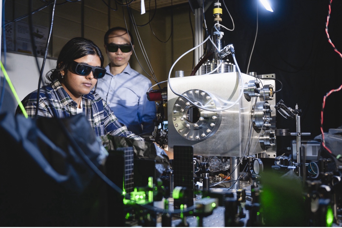
Saakshi Dikshit (left) and Tongcang Li working in the laboratory. (Photo by/Charles Jischke)
A Purdue University research team has developed a new quantum sensing device designed to look inside materials that usually block light, a step that could help scientists better understand what is happening inside lithium-ion batteries. The work addresses a central challenge in battery sensing. Many of the most important battery materials are difficult to study with optical quantum sensors. As Tongcang Li put it, "Opaque materials such as graphite, nickel, and lithium play critical roles in lithium-ion batteries and many other technological applications. However, sensing these materials using optical quantum sensors is challenging because they block light, limiting both excitation and signal collection."
The study, reported in Nano Letters, was led by Tongcang Li, a professor in the Department of Physics and Astronomy and in the Elmore Family School of Electrical and Computer Engineering at Purdue, in collaboration with researchers from Toyota. The Purdue team included PhD students Saakshi Dikshit, Sumukh Vaidya, Peng Ju, Kunhong Shen and Zhiyan Xie; postdoctoral researcher Xingyu Gao; and summer intern Troy Tsubota. The Toyota collaborators were Naveed Hussain, Shougo Higashi, Debasish Banerjee and Songtao Wu.
"In this project, we collaborated with scientists from Toyota to develop a device to use optically addressable quantum sensors for monitoring battery health," Dikshit said. That practical motivation sits behind a deeper physics problem. The team's sensor relies on spin defects in hexagonal boron nitride, or hBN, a two-dimensional material that can host quantum states sensitive to magnetic signals. These defects are promising for quantum sensing, but one drawback is that they are naturally dim, which makes collecting enough light difficult. Researchers often solve that by boosting the signal with plasmonic metal structures, but in opaque systems that can create a different problem. The sample blocks the light from one side, and the metallic structure blocks it from the other.
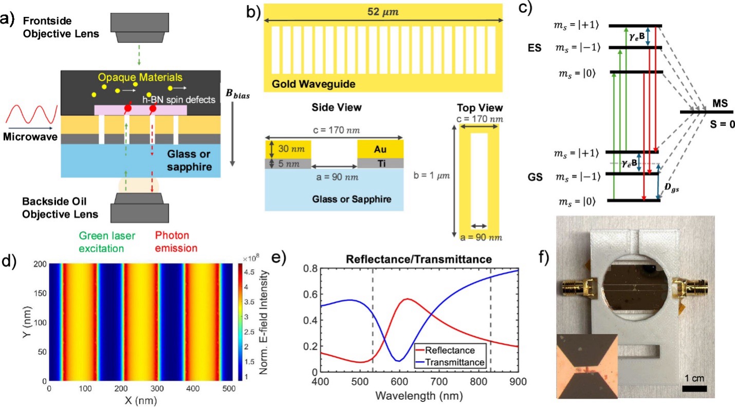
Figure 1. Proposed design for backward sensing of opaque materials using spin defects in hBN. (a) Schematic for the experimental setup. The waveguide consists of a 5 nm film of titanium and 30 nm film of gold fabricated on a 100–150 μm thick silica glass/sapphire coverslip. An oil immersion lens is used to collect photoemission from the backside of the device. (b) Schematic of the top and side views of the proposed nanoslit array. (c) Spin electronic structure of the defect. The ground state (GS) and excited state (ES) are spin S = 1 systems, with the metastable state (MS) being a singlet S = 0 system. Green arrows show 532 nm excitation; red arrows show spin-preserving radiative emission; and gray dotted arrows show spin non-conserving, non-radiative decay via the intersystem crossing (ISC). (d) COMSOL simulations showing the enhanced normalized E-field intensity within the nanoslits. The incident field is x-polarized. (e) Reflectance/transmittance through the nanoslit array for different wavelengths. The gray dashed lines mark the reflectance and transmittance through the nanoslit array at 532 and 830 nm. (f) Picture of the backside of the device. The device is attached to a plastic holder, enabling data collection from both sides. (Inset) Optical image of the microwave stripline. (Figure provided by/Saakshi Dikshit)
To get around that, the Purdue-led team designed a new kind of waveguide with a nanoslit array etched into a thin gold film. The slits are tiny openings, but they are enough to let light pass through the device from below while still preserving the plasmonic enhancement needed to strengthen the sensor's signal.
"To address this issue, we introduced a novel waveguide design featuring patterned nanoslit structures that enable light to pass through, allowing optical access to these opaque materials," Dikshit said. "The idea behind our device is like creating a tiny optical window in materials that normally block light, allowing us to observe their magnetic signals, which would otherwise be obstructed."
That idea is more than a design concept. The researchers showed that the nanoslit structure enhanced the local electric field by about 3.5 times at the relevant emission wavelength and increased the photoluminescence intensity by about 1.75 times compared with hBN placed on plain gold. The device also enabled backside optical access, meaning the team could excite the sensor and collect light through the substrate rather than through the opaque material sitting on top.
The researchers then demonstrated that the device worked in practice. They showed that the backside signal was strong enough to support continuous-wave optically detected magnetic resonance and pulsed measurements, both essential tools for quantum sensing. In one test, the frontside and backside measurements gave closely matched spin relaxation times, showing that the sensor could perform reliably even in the more difficult backside geometry.
For a proof of concept, the team tested the device with nickel nanoparticles, an opaque material relevant to battery systems. After the nanoparticles were placed on the device, frontside optical measurements were no longer possible because the material blocked the view. But the researchers could still read the quantum sensor from below through the nanoslit array. "We measure a 2D magnetic map of nickel nanoparticles as a proof-of-concept," Dikshit said.
The paper shows that when nickel nanoparticles were added, the quantum sensor's T1 spin relaxation time dropped from 12.6 microseconds to 8.8 microseconds, indicating that the device was detecting magnetic spin noise from the particles. The team also mapped the magnetic field of a nickel nanoparticle cluster in two dimensions, and the resulting field pattern closely matched the cluster's physical shape. In other words, the device did not just detect the presence of opaque particles. It spatially resolved their magnetic behavior.
That is where the technology starts to become especially interesting for industry. "The main industrial application of such a device can be to study electrochemical processes inside lithium-ion batteries," Dikshit said. "This device can also be used for chemical and biological sensing in opaque or scattering media." The paper makes the same broader point, noting that the device architecture could support in situ studies of electrochemical processes in lithium-ion batteries and other sensing applications in complex media.
Just as important, the team sees this as a beginning rather than an endpoint. "The next step in this research is to use this device to study the internal processes of a functioning battery," Dikshit said. That next phase could bring researchers closer to monitoring how batteries behave while they are actually operating, which could help improve performance, safety and lifetime.
The work also reflects the broader mission of Li's group at Purdue. "In our research group, we use spin qubits in 2D materials to study quantum interactions at the nanoscale to advance quantum sensing and quantum information science," Li said. "We also use optically levitated nanoparticles and nanodiamonds for precision measurements and studying macroscopic quantum mechanics.
Li said Purdue's research environment was essential to making the project possible. "This type of research at Purdue is aided by the Birck Nanotechnology Center," Li said. "For this project, we used the Zeiss Helium/Neon Focused Ion Beam and Photolihography facilities at BNC." Li is also a member of the Purdue Quantum Science and Engineering Institute, and the director of the Center for Quantum Technologies, a National Science Foundation Industry-University Cooperative Research Center. The technology developed in this work has been disclosed to the Purdue Innovates Office of Technology Commercialization and is patent-pending. The researchers also thanked the Toyota Research Institute of North America for funding the work.
About the Department of Physics and Astronomy at Purdue University
Purdue's Department of Physics and Astronomy has a rich and long history dating back to 1904. Our faculty and students are exploring nature at all length scales, from the subatomic to the macroscopic and everything in between. With an excellent and diverse community of faculty, postdocs and students who are pushing new scientific frontiers, we offer a dynamic learning environment, an inclusive research community and an engaging network of scholars.
Physics and Astronomy is one of the seven departments within the Purdue University College of Science. World-class research is performed in astrophysics, atomic and molecular optics, accelerator mass spectrometry, biophysics, condensed matter physics, quantum information science, and particle and nuclear physics. Our state-of-the-art facilities are in the Physics Building, but our researchers also engage in interdisciplinary work at Discovery Park District at Purdue, particularly the Birck Nanotechnology Center and the Bindley Bioscience Center. We also participate in global research including at the Large Hadron Collider at CERN, many national laboratories (such as Argonne National Laboratory, Brookhaven National Laboratory, Fermilab, Oak Ridge National Laboratory, the Stanford Linear Accelerator, etc.), the James Webb Space Telescope, and several observatories around the world.
Written by: David Siple, communications specialist, Purdue University Department of Physics and Astronomy