Heterostructures developed at Purdue support predictions of counterpropagating charged edge modes at the v=2/3 fractional quantum Hall state
2023-02-20
In 2018, a team of physicists at Purdue University invented a device which experimentally showed quasiparticles interfering for the first time in the fractional quantum Hall effect at filling factor v=1/3. Further development of these heterostructures has allowed the Manfra Group to expand their research to experiments that explore counterflowing charged edge modes at the 2/3 fractional quantum Hall state.
They have recently published their findings, “Half-Integer Conductance Plateau at the ν = 2/3 Fractional Quantum Hall State in a Quantum Point Contact,” in Physical Review Letters on February 17, 2023. This novel work has been selected as the Editor’s Suggestion for the forthcoming issue. Editor’s Suggestion articles are judged to be particularly important, interesting, and well written.
The team is led by Dr. Michael J. Manfra, Bill and Dee O’Brien Distinguished Professor of Physics and Astronomy, Professor of Electrical and Computer Engineering, Professor of Materials Engineering, and Scientific Director of the Microsoft Quantum Lab West Lafayette. The lead author of the publication is Dr. James Nakamura, senior research scientist. Dr. Geoffrey Gardner and graduate student Shuang Liang were also co-authors of this publication making valuable contributions to heterostructure growth.
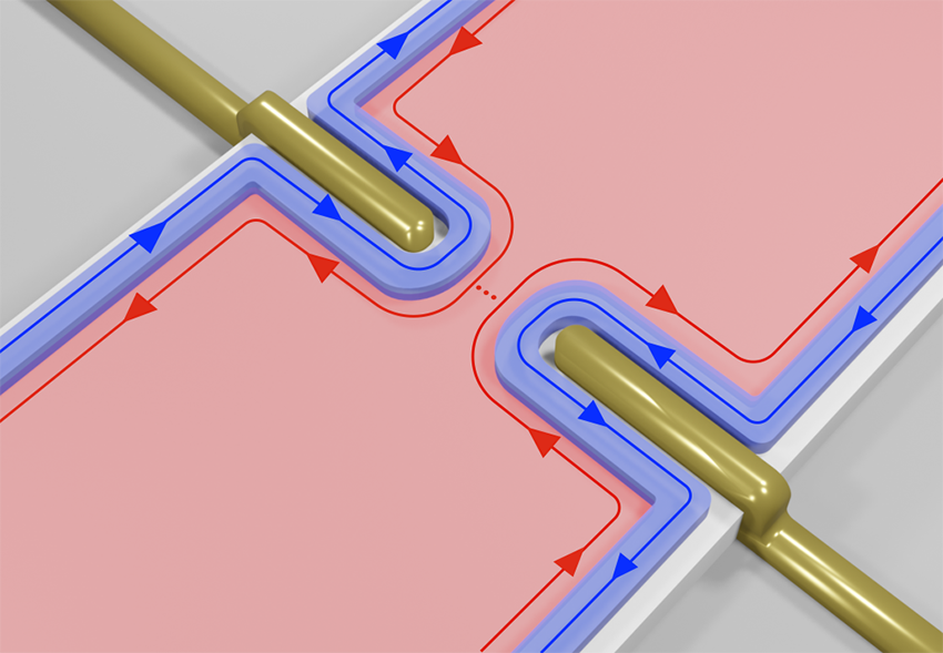
In the experiment, the team produced a semiconductor material which contains a sheet of two-dimensional electrons. On top of this semiconductor, they built a quantum point contact which consists of metal gates with a very narrow 300 nanometer gap. They used the quantum point contact to direct the conducting edge states through the narrow gap. In this configuration, demonstrated by the graphic above, they were able to measure an electrical conductance equal to half the fundamental value of e2/h. This experimental result is consistent with longstanding theoretical predictions for the edge states of the ν = 2/3 fractional quantum Hall state.
“We have a semiconductor structure that contains electrons arranged in a plane, called a two-dimensional electron system. When you cool the electrons down to low temperature and put them in a strong magnetic field, they form special states of matter called quantum Hall states,” explains Nakamura. “At a certain value of the magnetic field, the quantum Hall state is called the ν = 2/3 fractional quantum Hall state. At all quantum Hall states, electrical current is carried by edge states that flow around the edge of the sample, and they are chiral, meaning each edge state only flows in one direction (clockwise or counterclockwise). The ν = 2/3 state is predicted by theoretical physicists to have the special property that the there are two edge states which flow in the opposite direction to each other, one clockwise and the other counterclockwise. This is different from most quantum Hall states, where all the edge states flow in the same direction. We used a device with metal gates called a quantum point contact to control the edge states, and our measurements of the edge states in the quantum point contacts confirm the counterflowing edge states in our device. The quantum point contact brings the edge states on opposite edges of the sample close together. We measured a value of electrical conductance across the device equal to half of the value e2/h, where e is the electron’s charge and h is Planck’s constant. This value of the conductance is strong experimental evidence that our system has the edge structure with two counterflowing edge states.”
This all-Purdue team of physicists is uniquely set up for success at Purdue University due to state-of-the-art facilities spanning semiconductor growth, nanofabrication, and low temperature electrical measurements at the university.
“A crucial aspect is the nanotechnology facilities at Purdue,” says Nakamura. “This includes the machine, called an MBE (molecular beam epitaxy) machine, which is used to produce the semiconductor structures. This very specialized machine, operated by the Manfra group, requires expertise to build and operate so this is an essential advantage at Purdue. Liang, under the guidance of Gardner, is responsible for this aspect of our work. Additionally, the cleanroom in the Birck Nanotechnology Center is a state-of-the-art facility with a wide range of equipment available for us to use, that we used to fabricate the quantum point contact gates. Having all these resources and expertise available at one institution makes our experiments possible.”
This research is part of an ongoing quest to understand and manipulate fractionally charged anyons in fractional quantum Hall regime, a rich testbed for exploring the impact of topology in condensed matter physics which may possibly be used to create qubits.
This research is supported by the U.S. Department of Energy, Office of Science, Office of Basic Energy Sciences, under award number DE-SC0020138.
About the Department of Physics and Astronomy at Purdue University
Purdue Department of Physics and Astronomy has a rich and long history dating back to 1904. Our faculty and students are exploring nature at all length scales, from the subatomic to the macroscopic and everything in between. With an excellent and diverse community of faculty, postdocs, and students who are pushing new scientific frontiers, we offer a dynamic learning environment, an inclusive research community, and an engaging network of scholars.
Physics and Astronomy is one of the seven departments within the Purdue University College of Science. World-class research is performed in astrophysics, atomic and molecular optics, accelerator mass spectrometry, biophysics, condensed matter physics, quantum information science, particle and nuclear physics. Our state-of-the-art facilities are in the Physics Building, but our researchers also engage in interdisciplinary work at Discovery Park District at Purdue, particularly the Birck Nanotechnology Center and the Bindley Bioscience Center. We also participate in global research including at the Large Hadron Collider at CERN, Argonne National Laboratory, Brookhaven National Laboratory, Fermilab, the Stanford Linear Accelerator, the James Webb Space Telescope, and several observatories around the world.
About Purdue University
Purdue University is a top public research institution developing practical solutions to today’s toughest challenges. Ranked in each of the last five years as one of the 10 Most Innovative universities in the United States by U.S. News & World Report, Purdue delivers world-changing research and out-of-this-world discovery. Committed to hands-on and online, real-world learning, Purdue offers a transformative education to all. Committed to affordability and accessibility, Purdue has frozen tuition and most fees at 2012-13 levels, enabling more students than ever to graduate debt-free. See how Purdue never stops in the persistent pursuit of the next giant leap at https://stories.purdue.edu.
Written by Cheryl Pierce, Communications Specialist
Contributors: Dr. Michael J. Manfra and Dr. James Nakamura
Graphic by James Nakamura