Nanometer scale ohmic contact:
UHV STM images and current-voltage spectroscopic data
Reference:
Takhee Lee, et al, Appl. Phys. Lett. vol. 74, 2869 (1999).
Takhee Lee, et al, Appl. Phys. Lett.vol. 76, 212 (2000).
Overview
A requirement of many of nano-devices is the presence of nearby
contacts having dimensions of order 1 microns or greater. Thus, even
though the device has shrunk well into the nanometer-scale, the contacts to
the device still require areas of 102-104 greater than the active
device.
Therefore, nano-contacts having dimensions comparable to a nano-device
will be required to alleviate this difficulty in the future.
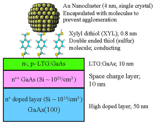
We have developed a nanometer-size, ohmic contacts to
n-type GaAs substrates. The nano-contacts are formed
between a single crystalline, nanometer-size Au cluster ( 4nm) and a GaAs
structure capped with layer of low-temperature-grown GaAs (LTG:GaAs).
A self-assembled monolayer of xylyl dithiol provides mechanical and electronic
tethering of the Au cluster to the LTG:GaAs surface.
The I(V) data of
the Au cluster/xylyl dithiol/GaAs show ohmic contact behavior with good
repeatability between various clusters distributed across the surface.
The specific contact resistance is determined to be
1 x 10⁻⁶ Ohm cm2.
Current densities above 1 x 10⁶ A/cm2 have been observed.
Schematic of nanoscale ohmic contact structure
The nanocontact structure contains:
4 nm Au cluster: Truncated octahedron single crystalline cluster.
Tether molecule: Xylyl dithiol (XYL) which is a double ended thiol molecule.
LTG:GaAs: Chemically stable, low resistance interface on GaAs
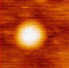
click to view high-resolution picture
25 x 25 nm UHV STM image of cluster on undoped LTG:GaAs surface.
The stability of the nano-contacts were
checked by performing 100 consecutive images over an 80 minute period
of time. From these measurements, the Au clusters were observed to remain stable and
did not exhibit any damage due to the scanning conditions employed.
These observations indicate that the clusters are well tethered to the
LTG:GaAs cap-layer.
The electronic properties of the Au nano-contacts were
investigated by measuring a series of I(V)s when the STM tip was
positioned over the Au cluster and over the XYL-coated
LTG:GaAs substrate.
When compared to the XYL-coated substrate, the
nano-contact is found to exhibit an ohmic behavior,
with a significant enhancement in the conduction for low bias voltages.
I-V over cluster (ohmic)
I-V over substrate (Non ohmic)
(Different curves represent different tip position over the sample.)

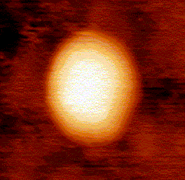
click to view high-resolution image
20 x 20 nm UHV STM image of cluster on p-doped LTG:GaAs surface.
Nano-ohmic contact behavior was also observed over Au nanocluster when p-doped LTG:GaAs cap layer was used.
I-V over cluster and substrate

click to view high-resolution image

Takhee Lee
Last modified: Sun Oct 10 12:45:57 EST 1999