What We're Doing:


Nanotube Nanotube research:
Electrical conduction through nanotubes
Electrostatic potential profile through nanotubes
Selected papers on nanotube research
Cluster Nanocluster research:
Electrical contact through nanocluster on semiconductor
Self-assembly of cluster network
Single electron tunneling through nanocluster
Selected papers on nanocluster research
/molecules Molecular wire research:
Electrical condcution through molecules
Selected papers on molecular wire research
Break Junction Break Junction research:
Quantized conductance of Au break junctions

Scanning Probe Microscopy

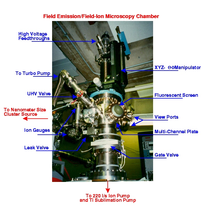
Scanning Probe Microscopy (SPM) is a process that is used to study the properties of surfaces at the atomic level. A Scanning Probe Microscope takes a probe that is atomically sharp and scans it over a surface, typically at a distance of a few angstroms or nanometers. In this research group, two different types of SPMs are used, an Atomic Force Microscope and a Scanning Tunneling Microscope.

Scanning Tunneling Microscopy

The Scanning Tunneling Microscope (STM) uses the quantum mechanical tunneling effect to determine the distance between the probe and the surface. Typically, the STM is set up to scan a surface at a constant distance away from the surface. Naturally, the probe will have to be moved up and down to follow the height of the surface, and this up and down motion can be used to make a three dimensional image of the surface.

Atomic Force Microscopy

The Atomic Force Microscope (AFM) uses various forces that occur when two objects are brought within nanometers of each other. An AFM can work either when the probe is in contact with a surface, causing a repulsive force, or when it is a few nanometers away, where the force is attractive. Scanning works similarly to the STM, and also creates three dimensional images.

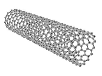
Electronic Properties of Carbon Nanotubes

Carbon nanotubes we discovered as early as 1975 (probably earlier), and TEM images of them were published by Endo et al.. In the wake of the Bucky-Ball (C60)fever, carbon nanotubes we "re-discovered" by Iijima (Nature 391, 1991). They represent real 1D systems for laboratory study. There has been much speculation about the physical and electronic properties of carbon nanotubes. As a natural extension of our expertise in nanoscale technology, we are using the techniques of field emission, STM, and transport measurements to study the electronic properties of carbon nanotubes. We have also developed a novel technique for making extremely good electrical contacts to the ends of a single nanotube (see Appl. Phys. Lett (APL) 74 p. 323-325.)


Field-Ion Microscopy (FIM)

Field-ion microscopy (FIM) can be used to study the structural properties of substances. A very sharp tip is placed inside a chamber containing a small amount of gas, usually hydrogen or helium, and pointed towards an imaging screen. A very high electric field is applied. As gas atoms near the tip are ionized they are drawn towards the screen by the electric field and an image of the surface of the tip is formed, typically with 2-5 angstrom resolution.


Back to Nanoscale Physics

People . Images . Papers . Experiments . Information


Takhee Lee
Last modified: Wed Dec 15 19:30:17 EST 1999