Patterned, 2-D array of close-packed 4 nm diameter Au clusters on
LTG:GaAs: SEM and STM images
Reference:
Jia Liu, et al, submitted to Appl. Phys. Lett. (2/2000).
Overview
Self-assembly techniques can offer the potential to
fabricate nanoscale elements without direct use of conventional
lithographic techniques, which become expensive and slow when used to
define nanoscale features.
The realization of electronic circuits of reasonable functionality
and complexity using self-assembly approaches
will require the ability to controllably
break the symmetry typically
found in self-assembled networks or to assemble the building
blocks (e.g. nanometer-size clusters) into specific configurations
as well as the ability to
realize devices with functionality comparable to current
semiconductor devices.
Toward the goal of a self-assembly technique which can
be used to realize robust electronic devices and circuits,
we have demonstrated
the fabrication of highly ordered
nanoscale elements defined in specific patterns using
a guided self-assembly technique on a semiconductor surface.
Specifically, we have developed a
process that allows high-quality close-packed arrays of
Au nanoclusters (5 nm in diameter)
to be formed in patterned regions on active GaAs substrates.
The local ordering at the nanometer scale is provided by a
chemically driven self-assembly process, while the arbitrary global
pattern is defined by the patterned template.
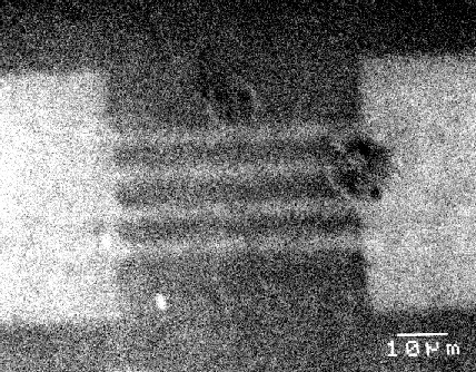
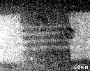
SEM (Scanning electron microscopy) image of patterned GaAs (LTG:GaAs) using stamp-pad
technique:
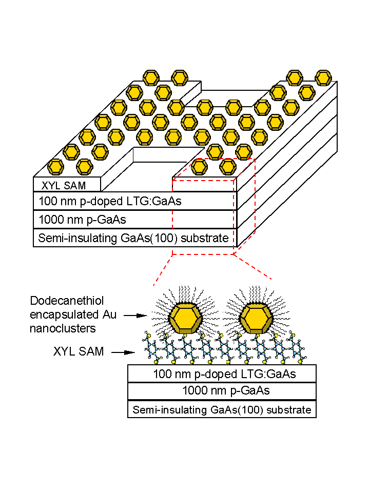
The directed self-assembly fabrication technique was used to form the
patterned cluster arrays involves (1) the deposition of an organic
tether molecule in pre-defined regions on the semiconductor substrate using
a microcontact printing technique, (2) the transfer
of a large-area (up to the centimeter length
scale) close-packed array of Au nanoclusters
onto the substrate, and (3) the removal of nanoclusters in the
regions not coated with the tether molecule.
The resulting structure is schematically illustrated here.
In the SEM image below, white region is bare LTG:GaAs and dark region is pattened region of 2-D array of
single-crystal Au clusters on LTG:GaAs substrate.
(This SEM image was taken by Prof. D. Janes in the School of
Electrical and Computer Engineering, Purdue University.)
click to view high-resolution image
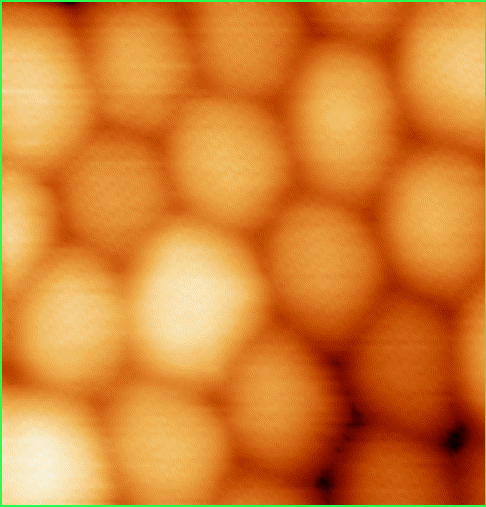
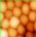
STM image of close-packed array of clusters in
patterned region.
When the STM tip was over the
Au nanocluster array (dark area in SEM image), hexagonal close-packed ordering was observed.
This high resolution image indicates that the interface layer of XYL provides a robust mechanical
tethering of the Au nanoclusters to the LTG:GaAs surface and
electronically links the Au clusters to the LTG:GaAs surface.
(30 x 30 nm UHV STM image was aquired with a sample voltage of -1.5 V, a set tunneling
current of 200 pA, and a scan rate of 2 Hz.)
click to view high-resolution image
Also, see TEM image of monolayer array of Au nanoclusters.

Takhee Lee
Last modified: Sun Oct 10 12:45:57 EST 1999