6th draft
S. Hong ![]() , D.B. Janes
, D.B. Janes ![]() , D. McInturff
, D. McInturff ![]() , R. Reifenberger
, R. Reifenberger ![]() and J.M. Woodall
and J.M. Woodall ![]()
![]() Purdue University, Department of Physics, W. Lafayette, Indiana 47907
Purdue University, Department of Physics, W. Lafayette, Indiana 47907
![]() Purdue University, School of Electrical and Computer
Engineering, W. Lafayette, Indiana 47907
Purdue University, School of Electrical and Computer
Engineering, W. Lafayette, Indiana 47907
![]() Purdue University, NSF MRSEC for Technology Enabling Heterostructure
Materials, W. Lafayette, Indiana 47907
Purdue University, NSF MRSEC for Technology Enabling Heterostructure
Materials, W. Lafayette, Indiana 47907
last modifications: Dec. 15, 1995
The stability of a GaAs layer structure consisting of a thin (10 nm) layer of low-temperature-grown GaAs on a heavily n-doped GaAs layer, both grown by molecular beam epitaxy, has been studied using a scanning tunneling microscope. The sample was exposed to the atmosphere between the layer growth and STM characterization. Tunneling spectroscopy shows both the GaAs band edges and a band of midgap states associated with the excess As in the surface layer. The observation of midgap states following atmospheric exposure indicates that the low-temperature-grown GaAs layer does not oxidize rapidly. The spectroscopy results are used to confirm a model for conduction in low resistance, nonalloyed contacts employing comparable layer structures.
Manuscript accepted for publication in Appl. Phys. Lett.
Low-temperature grown (LTG) GaAs, i.e. layers grown by molecular beam
epitaxy (MBE) at substrate temperatures of 250-300 ![]() C, has
been shown to possess a number of interesting electronic properties
associated with the excess arsenic concentration incorporated during
growth.[1] In as-grown LTG:GaAs material, the excess
arsenic results in a large concentration
C, has
been shown to possess a number of interesting electronic properties
associated with the excess arsenic concentration incorporated during
growth.[1] In as-grown LTG:GaAs material, the excess
arsenic results in a large concentration ![]() of point defects, due primarily to arsenic antisite
defects.[2, 3] The pinning of the Fermi level
near midgap in this material is generally associated with the point
defects.
of point defects, due primarily to arsenic antisite
defects.[2, 3] The pinning of the Fermi level
near midgap in this material is generally associated with the point
defects.
Recently, ex-situ low-resistance, nonalloyed contacts to n and
p-type GaAs have been demonstrated using a structure consisting of a
thin layer of LTG:GaAs (2-5 nm) on a highly doped layer of normal
growth temperature GaAs, both grown by MBE.[4] In this
study, specific contact resistances as low as ![]() have been reported on n-type GaAs
layers. The conduction model for the contact structure consisted of
defect assisted tunneling through the LTG:GaAs layer and tunneling
through the space charge region in the heavily doped layer. It was
postulated that the LTG:GaAs layer did not significantly oxidize during
prolonged exposure to the atmosphere because of the low surface
concentration of holes arising from the short minority carrier lifetime
in the LTG:GaAs material.[4] In order to evaluate the
suitability of the contact structure for device applications, it is
important to determine the stability of the surface layer following air
exposure.
have been reported on n-type GaAs
layers. The conduction model for the contact structure consisted of
defect assisted tunneling through the LTG:GaAs layer and tunneling
through the space charge region in the heavily doped layer. It was
postulated that the LTG:GaAs layer did not significantly oxidize during
prolonged exposure to the atmosphere because of the low surface
concentration of holes arising from the short minority carrier lifetime
in the LTG:GaAs material.[4] In order to evaluate the
suitability of the contact structure for device applications, it is
important to determine the stability of the surface layer following air
exposure.
As evidence for the instability of most GaAs surfaces, previous
STM spectroscopy studies on GaAs surfaces have
required special preparation procedures to avoid surface oxidation
and the associated loss of STM resolution. Cleaved
(110) surfaces have been prepared by either in-situ cleaving in an
ultra high vacuum (UHV) STM system or ex-situ cleaving followed by
sulfide passivation.[1, 2, 3, 5]
GaAs (001) surfaces passivated with As cap layers have been studied in
UHV STM experiments following removal of the As layer by heating in the
STM vacuum system.[6] STM spectroscopy has been performed on an unannealed layer of
LTG:GaAs (225 ![]() C) capped with a layer of GaAs grown at 350
C) capped with a layer of GaAs grown at 350 ![]() C.
Characterization of a (110) surface of the LTG:GaAs
layer exposed by cleaving in UHV
identified a band of midgap states associated
with the excess arsenic.[1, 2, 3] For
heavily doped n-type (n+) layers, this band of states was located above
the valence band edge of the material.
C.
Characterization of a (110) surface of the LTG:GaAs
layer exposed by cleaving in UHV
identified a band of midgap states associated
with the excess arsenic.[1, 2, 3] For
heavily doped n-type (n+) layers, this band of states was located above
the valence band edge of the material.
In order to characterize the stability of LTG:GaAs after air
exposure, STM spectroscopy studies were performed on a layer structure
comparable to the nonalloyed contact layers discussed above. While the STM
measurements were performed under UHV, the sample was exposed to the
atmosphere for a period of approximately 20 minutes during transfer
from the MBE system to the STM chamber. After initial measurements were
made, the sample was stored in a nitrogen filled desiccator for ![]() 25 hours to further study the effect of ambient on the mid-gap states
in LTG:GaAs. The observation of a band gap, along with a band of midgap
states above the valence band edge, confirms that the LTG:GaAs surface
layer does not significantly oxidize during atmospheric exposure and
confirms the defect-assisted tunneling model for the contact
structure.
25 hours to further study the effect of ambient on the mid-gap states
in LTG:GaAs. The observation of a band gap, along with a band of midgap
states above the valence band edge, confirms that the LTG:GaAs surface
layer does not significantly oxidize during atmospheric exposure and
confirms the defect-assisted tunneling model for the contact
structure.
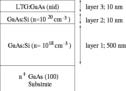
Figure 1: A schematic diagram of the GaAs structure investigated. The characterization of the
10 nm thick LTG:GaAs layer (layer 3) after exposure to ambient is of particular
interest.
The layer structure shown in Fig. 1 was grown in a Varian Gen II MBE on
an epi-ready n+ GaAs(100) substrate. The doped layers were grown at
the typical GaAs growth temperature of 580 ![]() C. The top
(undoped) layer was grown at 250
C. The top
(undoped) layer was grown at 250 ![]() C in order to incorporate
excess arsenic. The growth rate was 1
C in order to incorporate
excess arsenic. The growth rate was 1 ![]() m/hour. A silicon
filament was used to dope the layers n-type. This allows doping
concentrations of at least an order of magnitude higher than possible
with conventional effusion cells.
m/hour. A silicon
filament was used to dope the layers n-type. This allows doping
concentrations of at least an order of magnitude higher than possible
with conventional effusion cells.
It has been shown that the surface Fermi level is pinned near midgap during MBE growth of GaAs.[7] As a consequence, Si dopant atoms located within the surface carrier depletion region are incorporated primarily at donor sites, even for Si doping concentrations approaching the solid solubility limit. The presence of a LTG:GaAs cap layer maintains the high space charge density near the top of the heavily doped layer and therefore maintains the high concentration of activated donors within the region.
The wafer was unloaded and transferred in a vacuum package (P=50 millitorr) to the UHV STM apparatus so that it was exposed to air for the shortest possible amount of time. During transfer, the wafer was exposed to atmosphere for approximately 20 minutes.
The UHV STM used to characterize the LTG:GaAs layer is a homebuilt
system with a computer controlled digital feedback system, as
described elsewhere.[8, 9]
The base pressure
of the stainless steel vacuum chamber is below ![]() torr. The tips are etched Pt/Ir wires cleaned in the STM chamber by
field emission prior to use.
torr. The tips are etched Pt/Ir wires cleaned in the STM chamber by
field emission prior to use.
To investigate the uniformity of the LTG:GaAs layer, a few special
procedures were developed. Initially, large scale scans ( ![]() 300 nm
in extent) of the LTG:GaAs surface were taken in order to search for
localized non-uniformities. None were observed. In order to obtain
I(V) data at many locations, a scanning routine was developed that
periodically halted a normal topographic scan to obtain I(V) data.
Using this procedure, following the completion of a typical
topographic scan, an array of 10 x 10 I(V) curves were obtained. The
results presented here are from a typical topographic scan covering a
300 nm
in extent) of the LTG:GaAs surface were taken in order to search for
localized non-uniformities. None were observed. In order to obtain
I(V) data at many locations, a scanning routine was developed that
periodically halted a normal topographic scan to obtain I(V) data.
Using this procedure, following the completion of a typical
topographic scan, an array of 10 x 10 I(V) curves were obtained. The
results presented here are from a typical topographic scan covering a ![]() nm range. It follows that the set of 100 I(V) scans
obtained were approximately separated from each other by a
nm range. It follows that the set of 100 I(V) scans
obtained were approximately separated from each other by a ![]() nm lateral offset. By simultaneously acquiring an STM topograph, a
reliable procedure was implemented to guard against possible tip
crashes or tip switches while acquiring I(V) data. At each location,
a predetermined number (usually 70) of I(V) curves were taken and
averaged together to reduce noise. The averaged signal was used to
recover the local density of states at that location by calculating
dI/dV and I/V numerically from I(V).
nm lateral offset. By simultaneously acquiring an STM topograph, a
reliable procedure was implemented to guard against possible tip
crashes or tip switches while acquiring I(V) data. At each location,
a predetermined number (usually 70) of I(V) curves were taken and
averaged together to reduce noise. The averaged signal was used to
recover the local density of states at that location by calculating
dI/dV and I/V numerically from I(V).
In what follows, the density of states (DOS) is represented by
![]()
Dividing the differential conductivity dI/dV by I/V serves to
remove the slowly varying transmission function inherent in all I(V)
data, resulting in a quantity that more closely mirrors the desired
DOS. As suggested by Martensson and Feenstra, smoothing the
conductance (I/V) to reduce DOS features provides a better approximation to the tunneling
transmission function.[10] As discussed in Ref. 10, satisfactory
results were obtained by
smoothing the conductance with
a one pole, low-pass Fourier filter algorithm with a pole frequency
specified by ![]() . By choosing
. By choosing ![]() larger than
larger than ![]() ,
the semiconductor gap, the low-pass Fourier filter suppresses DOS features
within the band gap. As a result, the transmission function (which
should not depend on the gap structure) can be recovered to a better
approximation. In this way, Feenstra et al. were able to recover
reliable electronic spectra of GaAs containing arsenic-related point
defects.[11] Since the bulk GaAs gap is
,
the semiconductor gap, the low-pass Fourier filter suppresses DOS features
within the band gap. As a result, the transmission function (which
should not depend on the gap structure) can be recovered to a better
approximation. In this way, Feenstra et al. were able to recover
reliable electronic spectra of GaAs containing arsenic-related point
defects.[11] Since the bulk GaAs gap is ![]() 1.43 eV, in this study
the differential conductance (dI/dV) was normalized using the conductance
(I/V) broadened by a low-pass Fourier filtering with a cutoff frequency
of
1.43 eV, in this study
the differential conductance (dI/dV) was normalized using the conductance
(I/V) broadened by a low-pass Fourier filtering with a cutoff frequency
of ![]() .
.
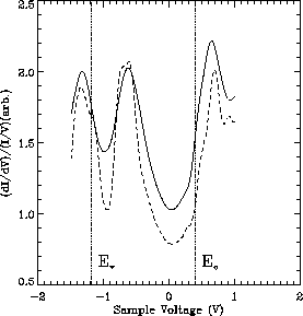
Figure 2: Normalized conductance of LTG:GaAs as a function of sample voltage
after 20 minutes
exposure to ambient. The dashed line is a typical set of data obtained
at an arbitrary location of the Pt/Ir tip.
The solid line is the average of data obtained
from 100 different spatial locations in ![]() area.
area.
Fig. 2 shows the normalized conductance obtained after 20
minutes exposure to ambient air. The dashed line is a representative
scan at a specific spatial location, while the solid line is the
average of the scans at 100 spatial locations in ![]() nm
area. The effective conduction and valence band edges (marked by
nm
area. The effective conduction and valence band edges (marked by ![]() and
and
![]() ), along with a band of gap states near the valence band edge are
observed. In order to have a well-defined criterion for locating the band edges,
the inflection point determined from the second derivative of I(V) was used to define
an effective band edge.
Although this procedure probably overestimates the size of the band-gap, it does
provide a reliable way to compare band-gaps from I(V) data obtained at different
locations. Following this procedure, the
measured effective gap was found to be 1.58eV in Fig. 2, a value
slightly larger than the band gap of bulk GaAs (1.43eV). From Fig. 2,
the gap states are centered at a sample bias
voltage near -0.64V. Using the valence band edge as a reference, this
translates into a state located 0.54 eV above the effective valence band edge. The
location of this feature is similar to the one observed in
UHV-cleaved, n-doped LTG:GaAs.[2, 3]
), along with a band of gap states near the valence band edge are
observed. In order to have a well-defined criterion for locating the band edges,
the inflection point determined from the second derivative of I(V) was used to define
an effective band edge.
Although this procedure probably overestimates the size of the band-gap, it does
provide a reliable way to compare band-gaps from I(V) data obtained at different
locations. Following this procedure, the
measured effective gap was found to be 1.58eV in Fig. 2, a value
slightly larger than the band gap of bulk GaAs (1.43eV). From Fig. 2,
the gap states are centered at a sample bias
voltage near -0.64V. Using the valence band edge as a reference, this
translates into a state located 0.54 eV above the effective valence band edge. The
location of this feature is similar to the one observed in
UHV-cleaved, n-doped LTG:GaAs.[2, 3]
>From the array of I(V) data, it is also possible to assess the integrity of the LTG:GaAs layer. In 88 of the 100 scans taken at different spatial locations, evidence for a clear gap state peak is found. In the other 12 scans, noisy data resembling the GaAs band gap was observed. The spatial distribution of midgap state density is consistent with the previous reports of defect densities in LTG:GaAs.[1, 2, 3]
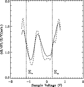
Figure 3: Normalized conductance of LTG:GaAs as a function of sample voltage
after 25 hours of storage in a nitrogen filled desiccator.
The dashed line is a typical set of data obtained
at an arbitrary location of the Pt/Ir tip. The solid line is the average
of data obtained from 100 different spatial locations in ![]() area.
area.
During the course of the measurements described above, the sample was
stored in the UHV chamber for a period of ![]() 3 weeks. During this
time, no significant degradation of the mid-gap states was detected. In
order to further assess the stability of the mid-gap states in the
LTG:GaAs layer, the sample was removed from the UHV chamber and stored
in a nitrogen filled desiccator for 25 hours. Fig. 3
shows the data obtained after reinserting the sample into the UHV STM
chamber. The GaAs band edges as well as the gap states can be readily
resolved without dramatic change. This data shows that the electronic
properties of the structure are stable and convincingly supports the
claim that LTG:GaAs does not rapidly oxidize upon exposure to air.
3 weeks. During this
time, no significant degradation of the mid-gap states was detected. In
order to further assess the stability of the mid-gap states in the
LTG:GaAs layer, the sample was removed from the UHV chamber and stored
in a nitrogen filled desiccator for 25 hours. Fig. 3
shows the data obtained after reinserting the sample into the UHV STM
chamber. The GaAs band edges as well as the gap states can be readily
resolved without dramatic change. This data shows that the electronic
properties of the structure are stable and convincingly supports the
claim that LTG:GaAs does not rapidly oxidize upon exposure to air.
In summary, this study supports the claim of a reduced oxidation of
LTG:GaAs when exposed to ambient conditions. This remarkable behavior
was previously invoked to explain the ohmic contact experiments on a
similar sample structure with a thinner ( ![]() nm ) LTG:GaAs layer
by Patkar et al.[4] A reduced contact resistance was
observed and was explained by a defect-assisted tunneling mechanism
through the LTG:GaAs. In the present study, we find that the
normalized conductance shows an enhanced gap state, centered at 0.54
eV above the effective valence band edge. The location of this state
is consistent with the results of Feenstra et al. obtained from a
cleaved LTG:GaAs layer.[2, 3] Data taken after
20 minutes exposure to ambient, after
nm ) LTG:GaAs layer
by Patkar et al.[4] A reduced contact resistance was
observed and was explained by a defect-assisted tunneling mechanism
through the LTG:GaAs. In the present study, we find that the
normalized conductance shows an enhanced gap state, centered at 0.54
eV above the effective valence band edge. The location of this state
is consistent with the results of Feenstra et al. obtained from a
cleaved LTG:GaAs layer.[2, 3] Data taken after
20 minutes exposure to ambient, after ![]() 3 weeks in a UHV chamber,
and after 25 hours storage in a nitrogen filled desiccator show no
degradation of this gap state and suggest that reliable electrical
contacts to buried GaAs-based heterostructures are now possible using
this LTG:GaAs as a contact intermediate.
3 weeks in a UHV chamber,
and after 25 hours storage in a nitrogen filled desiccator show no
degradation of this gap state and suggest that reliable electrical
contacts to buried GaAs-based heterostructures are now possible using
this LTG:GaAs as a contact intermediate.
This work was partially supported by the NSF MRSEC program under Grant 9400415-DMR and the Army Research Office URI program under Contract DAAL03-G-0144. We would like to thank V. R. Kolagunta, T. P. Chin and Prof. M. R. Melloch for helpful discussions.
 Back to Nanoscale Physics page