Novel Infrared Optical Materials Based on III-Nitride Semiconductors: Growth, Structure and Properties
This project investigates fundamental materials issues of a new class of complex materials containing two or more metal nitrides. These materials are interesting because of their potential use in novel optoelectronic devices of importance for technological applications beneficial to society (sensing, imaging, and telecommunications). Due to their widely dissimilar physical and chemical properties, these complex compounds form a variety of unique nanostructures when grown together in thick stacks of many layers. This project aims to understand, control, and tailor the local atomic arrangement of the materials at the nanoscale to maximize light absorption in the invisible infrared range. The project also explores the effect of nanostructure on local transfer of free electrical charge. Of particular interest is the impact of the crystal orientation on optical and electrical properties.
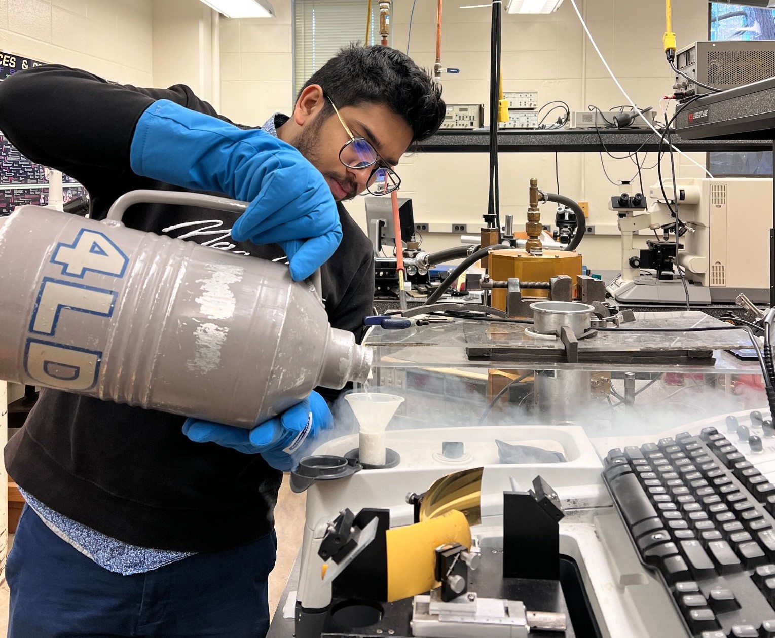
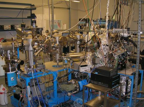
The principal objective of this project is to establish the relationship between growth, atomic structure and infrared optical properties of AlIn(Ga)N/(In)GaN multi-quantum well structures grown by plasma-assisted molecular beam epitaxy on c- and m-plane GaN. The project particularly focuses on unraveling the impact of nanostructure on infrared intersubband absorption, a property that is essential for the application of these materials in novel infrared optoelectronics (emitters and detectors). The research effort involves material design and growth, as well as structural and optical material characterization of AlIn(Ga)N/(In)GaN heterostructures. The growth of nitride heterostructures advances the state-of-the-art in nitride epitaxy. In order to correlate the nanostructure with optical properties, the atomic structure of the semiconductor materials is characterized in detail using high-resolution x-ray diffraction and transmission electron microscopy, while the infrared optical properties of the materials are examined experimentally using Fourier transform infrared spectroscopy. A secondary goal is to develop predictive material modeling capabilities that enable conduction-band engineering for light emission.