Mesoscopic Point-Like Defects in Semiconductors
Mesoscopic point-like defects are a class of extended defects
with surfaces of minimal curvature that span in size from the
point defect limit (multi-vacancy, antisite, impurity complex,
etc.) to macroscopic inclusions or voids within a semiconductor
host. The structural, electronic and optical properties of these
defects evolve continuously from the quantum-mechanical limit
to the classical limit. Mesoscopic defects share some features
in common with quantum dots, such as Coulomb charging energies,
but unlike quantum dots their electronic properties are dominated
by the covalent bond energies of the defect-semiconductor interface.
The deep-level energies of spheroidal mesoscopic defects are
calculated self-consistently in the unrestricted Hartree-Fock
approximation using an extension of the many-electron model of
Haldane and Anderson. The calculations in GaAs reveal a high-multiplicity
Coulomb ladder of discrete charge states distributed across the
semiconductor band gap and centered on the charge neutrality level.
The history of semiconductor research over the past century has been characterized by steadily increasing material heterogeneity. The first half century concentrated on bulk crystals of elemental and compound semiconductors, while the later half saw forays into epitaxy. Epitaxy evolved from simple homoepitaxy into more sophisticated forms, culminating in the versatile heteroepitaxy of molecular beam epitaxy and related growth techniques. Today, semiconductor heteroepitaxy is continuing to evolve, expanding beyond all-semiconductor heterostructures to include metal-semiconductor [1], insulator-semiconductor, and superconductor-semiconductor heterostructures and composites [2]. With the proliferation of diverse new forms of heterogeneous composite materials, it is important to identify unifying principles and concepts that encompass the physics of a wide range of seemingly unrelated materials within a single class.
For instance, the physical properties of inclusions within semiconductors may be viewed as a single class of mesoscopic defect that includes the simple limit of point defects as well as the electronic properties of extended defects. The accumulation of vacancies into increasingly larger multi-vacancy complexes is perhaps the best example of the continuous extension from the point defect limit (the isolated vacancy) to the mesoscopic limit (voids) [3]. Impurity atoms or nonstoichiometric concentrations can also accumulate into precipitates within the semiconductor [1]. These voids and precipitates are mesoscopic point-like defects that exchange charge with the semiconductor host and have well-defined 'deep-level' energies.
The term 'mesoscopic' describes those defects that have a characteristic energy scale that brings them continuously from the point defect (quantum) limit to the classical limit. This characteristic energy is the Coulomb charging energy, reduced by hybridization with the semiconductor host. Mesoscopic defects have Coulomb charging energies comparable to or smaller than the semiconductor bandgap. The term 'point-like' describes defects that are primarily spheroidal, with possible faceting. They are unlike other extended defects, such as line defects (dislocations, etc.) or plane defects (platelets, stacking faults, etc.), because point-like defects have bulk volumes enclosed by surfaces of minimal curvature. The small curvature minimizes Coulomb energies and maximizes the number of charge states that can exist within the semiconductor bandgap.
Mesoscopic point-like defects retain many of the features of point defects, such as the presence of discrete charge state energy levels within the semiconductor bandgap, and their ability to participate in compensation mechanisms within the semiconductor. But they also have important differences from point defects, such as extremely high charge-state multiplicity. It is the high multiplicity, in particular, that makes these mesoscopic point-like defects important constituents in compensated semiconductors.
The importance of mesoscopic defects for charge compensation was proposed by Warren et al. [4] to explain the semi-insulating properties of nonstoichiometric GaAs. Nonstoichiometric GaAs forms during molecular beam epitaxy on substrates held at low temperatures (near 200 - 300 oC) rather than at the usual growth temperature of 600 oC. Low-temperature-growth (LTG) incorporates excess arsenic into the GaAs [5, 6] . A key discovery by Purdue researchers was that the excess arsenic undergoes precipitation into small arsenic inclusions upon post-growth anneal [7]. The accumulation process and size of the precipitate is controlled by growth or post-growth material processing [1]. Therefore, the precipitates could be 'engineered', and their size and spacing could be controlled and chosen simply by playing off growth temperature against anneal temperature and time [8]. Nonstoichiometric GaAs and related compounds are semi-insulating under most growth and post-growth processing conditions and are playing an increasingly important technological role. They are currently being developed as ultrafast photodetectors [9, 10] with sub-picosecond lifetimes [11], as far-infrared photodetectors [12], in the fabrication of GaAs-based integrated circuits [13], and in photorefractive quantum wells [14, 15, 16], among other applications.
Since the discovery of the arsenic precipitates, the semi-insulating nature of nonstoichiometric GaAs had been a source of controversy, until recently. The semi-insulating properties were initially attributed to the high concentration of arsenic-related point defects [17]. Warren et al. [4] proposed that the arsenic precipitates were acting as internal Schottky barriers with associated depletion regions surrounding the precipitates. Subsequent studies have supported either the defect or the Schottky models, depending on the growth and anneal conditions. The production of mesoscopic voids in heavily radiation-damaged GaAs [3] raised a complication in the defect vs. Schottky argument because these voids cannot be viewed as Schottky barriers with a high density of available internal states. However, the materials with the voids are semi-insulating with many of the same properties as nonstoichiometric GaAs containing arsenic precipitates. It was shown recently that the voids play virtually an identical role as the precipitates for their ability to compensate charge [18], and that voids and precipitates can be viewed within a broader class of mesoscopic point-like defects that share many common properties, independent of their internal constituents.
Because the energy levels of mesoscopic point-like defects in semiconductors attain high charge multiplicity, they must be calculated within a many-electron theoretical framework. One simple many-electron model that has been a valuable heuristic tool is the model of Haldane and Anderson [19]. This model was originally developed to explain the occurrence of multiple charge states of transition-metal impurities in semiconductors. It was later used to calculate effective U properties of the dangling bond in silicon [20], and to explain the band lineup of heterostructures with respect to transition metal energy levels [21]. More recently, it has been used to calculate the charge state splitting of deep energy levels in narrow-gap semiconductors [22], to track the formation of Schottky barriers by atoms adsorbed on a semiconductor surface [23], and to explain the compensation of doped semiconductors by mesoscopic voids [18].
We extend the Haldane-Anderson model to calculate the deep energy
levels of mesoscopic point-like defects in GaAs. Two extensions
to the Haldane-Anderson model are necessary. First, the intrasite
Coulomb interaction energy U is identified. This is done in a
manner that is consistent with both the classical limit of the
charging energy of a classical metallic sphere, as well as with
the point defect limit. The second extension to the model is
the identification of the role played by the charge neutrality
level [24]. The neutral mesoscopic defect level coincides with
the charge neutrality level of the semiconductor bandstructure.
This behavior is included explicitly into the many-electron model.
These two extensions are described in section II. In section
III, the calculations are presented for the deep energy levels
for both spherical, as well as spheroidal defects. The classical
limit is discussed in section IV as the limiting behavior for
large defect radius.
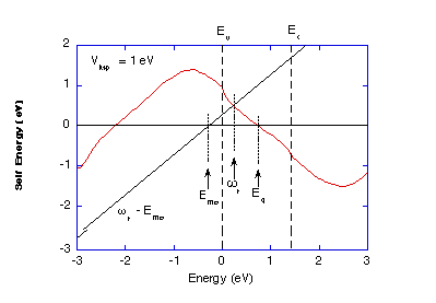
Fig. 1 Graphical solution to find the occupied pole in the bandgap
for a defect energy Ems.
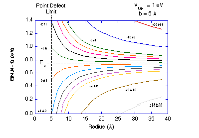
Fig. 2 Deep-level energies of spherical voids corrected for long-range
potentials with b = 5 Å showing the development of the Coulomb
ladder.
1M. R. Melloch, J. M. Woodall, E. S. Harmon, N. Otsuka, F. Pollak, D. D. Nolte, R. M. Feenstra and M. A. Lutz, Low-Temperature-Grown III-V Materials in Annual Review of Material Science, 25, B. W. Wessels, ed., (Annual Reviews, Inc., Palo Alto, 1995)2M. L. Cohen, Phys. Scr. Vol. T T68, 84 (1996)3W. Walukiewicz, Z. Lilienthal-Weber, J. Jasinski, M. Almonte, A. Prasad, E. E. Haller, E. R. Weber, P. Grenier and J. F. Whitaker, Appl. Phys. Lett. 69, 2569 (1996)4A. C. Warren, J. M. Woodall, J. L. Freeouf, D. Grischowsky, D. T. McInturff, M. R. Melloch and N. Otsuka, Appl. Phys. Lett. 57, 1331 (1990)5K. Mahalingam, N. Otsuka, M. R. Melloch, J. M. Woodall and A. C. Warren, J. Vac. Sci. Technol. B 9, 2328 (1991)6Z. Lilienthal-Weber, A. Claverie, J. Washburn, F. W. Smith and A. R. Calawa, Appl. Phys. A 53, 141 (1991)7M. R. Melloch, N. Otsuka, J. M. Woodall, A. C. Warren and J. L. Freeouf, Appl. Phys. Lett. 57, 1531 (1990)8M. R. Melloch, J. M. Woodall, N. Otsuka, K. Mahalingham, C. L. Chang and D. D. Nolte, Mat. Sci. and Eng. B22, 31 (1993)9F. W. Smith, H. Q. Le, V. Diadiuk, M. A. Hollis, A. R. Calawa, S. Gupta, M. Frankel, D. R. Dykaar, G. A. Mourou and T. Y. Hsiang, Appl. Phys. Lett. 54, 890 (1989)10A. C. Warren, N. Katzenellenbogen, D. Grischkowsky, J. M. Woodall, M. R. Melloch and N. Otsuka, Appl. Phys. Lett. 58, 1512 (1991)11Gupta, Appl. Phys. Lett. 59, 3276 (1991)12A. Srinivasan, K. Sadra, J. C. Campbell and B. G. Streetman, J. Electron. Mat. 22, 1457 (1993)13F. W. Smith, A. R. Calawa, C.-L. Chen, M. J. Mantra and L. J. Mahoney, IEEE Electron. Dev. Lett. EDL-9, 77 (1988)14I. Lahiri, K. M. Kwolek, D. D. Nolte and M. R. Melloch, Appl. Phys. Lett. 67, 1408 (1995)15I. Lahiri, M. Aguilar, D. D. Nolte and M. R. Melloch, Appl. Phys. Lett. 68, 517 (1996)16I. Lahiri, D. D. Nolte, M. R. Melloch and M. B. Klein, Optics Lett. 23, 49 (1998)17M. Kaminska, E. R. Weber, Z. Liliental-Weber and R. Leon, J. Vac. Sci. Technol. B7, 710 (1989)18D. D. Nolte, Appl. Phys. Lett. 70, 3401 (1997)19F. D. M. Haldane and P. W. Anderson, Phys. Rev. B 13, 2553 (1976)20W. B. Fowler and R. J. Elliott, Phys. Rev. B 34, 5525 (1986)21M. Hamera, W. Walukiewicz, D. D. Nolte and E. E. Haller, Phys. Rev. B 39, 10114 (1989)22W. Li and J. D. Patterson, Phys. Rev. B 53, 15622 (1996)23S. Y. Davydov, Semiconductors 31, 1062 (1997)24W. Mönch, Semiconductor Surfaces and Interfaces (BErlin, Springer-Verlag, 1995)