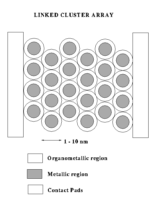
 FIG. 1:
A schematic diagram of a simple linked cluster array.
FIG. 1:
A schematic diagram of a simple linked cluster array.
FIG. 1:
A schematic diagram of a simple linked cluster array.
In order to circumvent these two problems, an interdisciplinary group of researchers at Purdue University is trying a different approach to the fabrication of two-dimensional electronic devices. The approach they are following relies on the construction of electronically interesting structures utilizing principles of self-assembly. First, a uniform population of nanometer diameter metal clusters are synthesized and then assembled into patterned arrays on a flat insulating substrate. After assembly, the clusters are interconnected with conductive organic molecules, forming a linked cluster array. A schematic representation of such an array is shown in Figure 1.
The first step in this process is achieved by growing the metal clusters as aerosol particles in a unique gas aggregation reactor developed by R.P. Andres and his students in the School of Chemical Engineering. This Multiple Expansion Cluster Source (MECS) produces an aerosol stream containing metal clusters entrained in an inert gas. The mean diameter of the clusters can be controlled in the range from 1-20 nm with a narrow size distribution. Once formed, the clusters are annealed in flight to yield perfect single crystal particles. In the case of gold, the clusters form fcc crystals with the overall shape of a truncated octahedron.[1]
The next step is to adsorb a monolayer of a surface active organic molecule onto these nanocrystals to prevent aggregation before deposition on a flat substrate. This is accomplished by contacting the metal particle aerosol with an organic solvent such as decane or 1,3,5-trimethylbenzene that contains a suitable surfactant species. In the case of gold clusters it is found that an alkyl thiol such as 1-dodecanethiol is ideal for encapsulating the clusters and preventing them from aggolomerating. Once the clusters have been captured in an organic solvent and encapsulated by surfactant they can be stored as stable colloids for months.
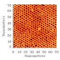 FIG. 2:
A TEM micrograph of a close-packed monolayer array of Au
clusters supported on a thin flake of
MoS_2.
All the clusters are encapsulated by a layer of dodecanethiol.
FIG. 2:
A TEM micrograph of a close-packed monolayer array of Au
clusters supported on a thin flake of
MoS_2.
All the clusters are encapsulated by a layer of dodecanethiol.
When a dilute solution of encapsulated clusters is spread onto an atomically smooth substrate, the clusters spontaneously assemble into close-packed arrays. Uniform two-dimensional arrays measuring several microns in diameter can be formed in this way. Figure 2 is a bright field transmission electron microgaph of a section of such an array. This close packed structure is made up of 4 nm diameter gold clusters encapsulated using 1-dodecanethiol and cast on a thin crystal of MoS_2.
The last step in fabricating an electronically interesting two-dimensional cluster array is to interconnect a network of clusters with ``molecular wires''. These wires must satisfy three criteria. First, they must contain functional groups that have a proven affinity for covalently bonding to metals. Thiols have been shown to be particularly effective in this regard. Alkyl thiols form ordered, durable monolayer films anchored by the sulfer atoms to flat gold surfaces.[2,3] Isonitrile groups also chemisorb strongly to many metals. Second, the molecular wires should form an electronically conjugated system, with strong electronic coupling from end to end. In general, the most suitable candidates to meet this criteria are small oligomeric structures of proven conducting polymers. Finally, the molecular wires must be double-ended to promote the linking or interconnection of adjacent clusters.
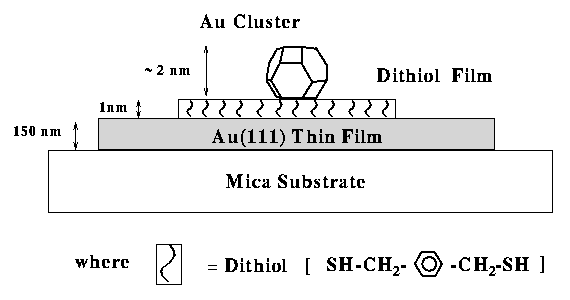
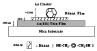 FIG. 3:
Schematic of the single electron tunneling experiment performed at room
temperature.
FIG. 3:
Schematic of the single electron tunneling experiment performed at room
temperature.
Several candidate ``molecular wires'' have been synthesized by C.P. Kubiak and his students in the Chemistry Department. These molecules have oligomeric structures related to polyphenylene and polyphenylene-acetylene with thiol or isonitrile end groups. They have shown that it is possible to prepare a self assembled monolayer (SAM) of the double-ended thiols (dithiols), biphenyldithiol (BPD) and xylyldithiol (XYL), in which only one end of the molecule bonds to an atomically flat gold surface.[4] Furthermore, each of these two dithiols is found to spontaneously displace a preexisting SAM of 1-octadecanethiol on a gold substrate. Such chemical substitution provides a simple way to covalently form a two-dimensional cluster array.
R. Reifenberger and his students in the Physics Department are measuring the electrical conductivity of cluster-based nanostructures utilizing scanning tunneling microscope (STM) techniques. In initial experiments a SAM of XYL was prepared on an atomically flat gold substrate and annealed gold clusters were deposited in vacuum onto the XYL covered substrate as shown schematically in Figure 3. The XYL molecules tethered the gold clusters to the underlying substrate, allowing reproducible STM scans of the clusters.[5]
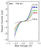
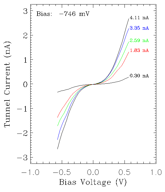
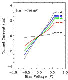 FIG. 4:
Left:
I(V) data through a single nanometer-size cluster supported by XYL
molecular wires.
Right:
I(V) data when the tip is positioned over the XYL covered
substrate. The data were obtained in vacuum at room temperature.
FIG. 4:
Left:
I(V) data through a single nanometer-size cluster supported by XYL
molecular wires.
Right:
I(V) data when the tip is positioned over the XYL covered
substrate. The data were obtained in vacuum at room temperature.
Because of the long-term stability of the sample, it was possible to obtain reliable I(V) spectra using an STM tip positioned over a single cluster and over the XYL film. When the tip is over a cluster, suppression of the tunnel current at zero bias voltage (Coulomb blockade) and reproducible steps (Coulomb staircase) are found. When the tip is over the dithiol film, a linear I(V) results. Typical I(V) data are shown in Figure 4. Analysis of the I(V) spectra, using a standard model for a double-junction tunnel capacitor, yields reasonable values for the capacitances (~10^-19 F to ~10^-20 F) expected from the known geometry. From these measurements an estimate for the resistance of a single XYL molecule of approximately 125 megaohms was obtained.[5] This result is in agreement with the resistance estimated from a theoretical model developed by S. Datta (School of Electrical Engineering), C.P. Kubiak and their students. The resistance is calculated from the Landauer formula
 .
.Although other measurements of room temperature Coulomb blockade have been serendipitously observed and reported, this is believed to be the first time that the structure giving rise to the single electron tunneling behavior has been well characterized.
Based on the promising results obtained in the experiments described above, monolayer arrays of encapsulated gold clusters have been deposited in the gap between two gold pads fabricated on an amorphous SiO_2 surface by D.B. Janes and his students in the School of Electrical Engineering. The resulting array is immersed in a solution containing BPD to electronically link the clusters to each other and to the gold contact pads. While these first experiments are still inconclusive, some samples have yielded I(V) curves exhibiting a gap at low bias voltages and a sharp rise in conduction at high bias voltages as might be expected.[6]
In conclusion, many of the steps necessary for the fabrication of patterned networks of electronically linked, two-dimensional arrays of gold clusters have been successfully carried out. More work is required to determine whether the approach developed provides a viable method for constructing robust networks of coupled, nanometer-size metal clusters. The results to date, however, appear promising. Already it is apparent that nanoscale gold clusters linked by organic molecules represent an interesting model system to study single electron tunneling in molecular nanostructures at room temperature. Adjusting the size of the clusters and the degree of coupling between them should yield a broad range of useful electronic properties.